- 您现在的位置:买卖IC网 > Sheet目录1994 > DS3106LN+ (Maxim Integrated Products)IC TIMING LINE CARD 64-LQFP
DS3106
27
7.8.2.3 OC3 and OC6 Configuration
The following is a step-by-step procedure for configuring the frequencies of output clocks OC3 and OC6:
Use Table 7-8 to select a set of output frequencies for each APLL, T0 and T4. Each APLL can only
generate one set of output frequencies. (In SONET/SDH equipment, the T0 APLL is typically
configured for a frequency of 311.04MHz to get N x 19.44MHz output clocks to for use on line cards.)
Determine from Table 7-8 the T0 and T4 APLL frequencies required for the frequency sets chosen in step
2.
in Table 7-11 for the T4 APLL frequency determined in step 3.
Using Table 7-8 and Table 7-12, configure the frequencies of output clocks OC3 and OC6 in the OFREQn
Table 7-13 lists all standard frequencies for the output clocks and specifies how to configure the T0 APLL and/or
the T4 APLL to obtain each frequency. Table 7-13 also indicates the expected jitter amplitude for each frequency.
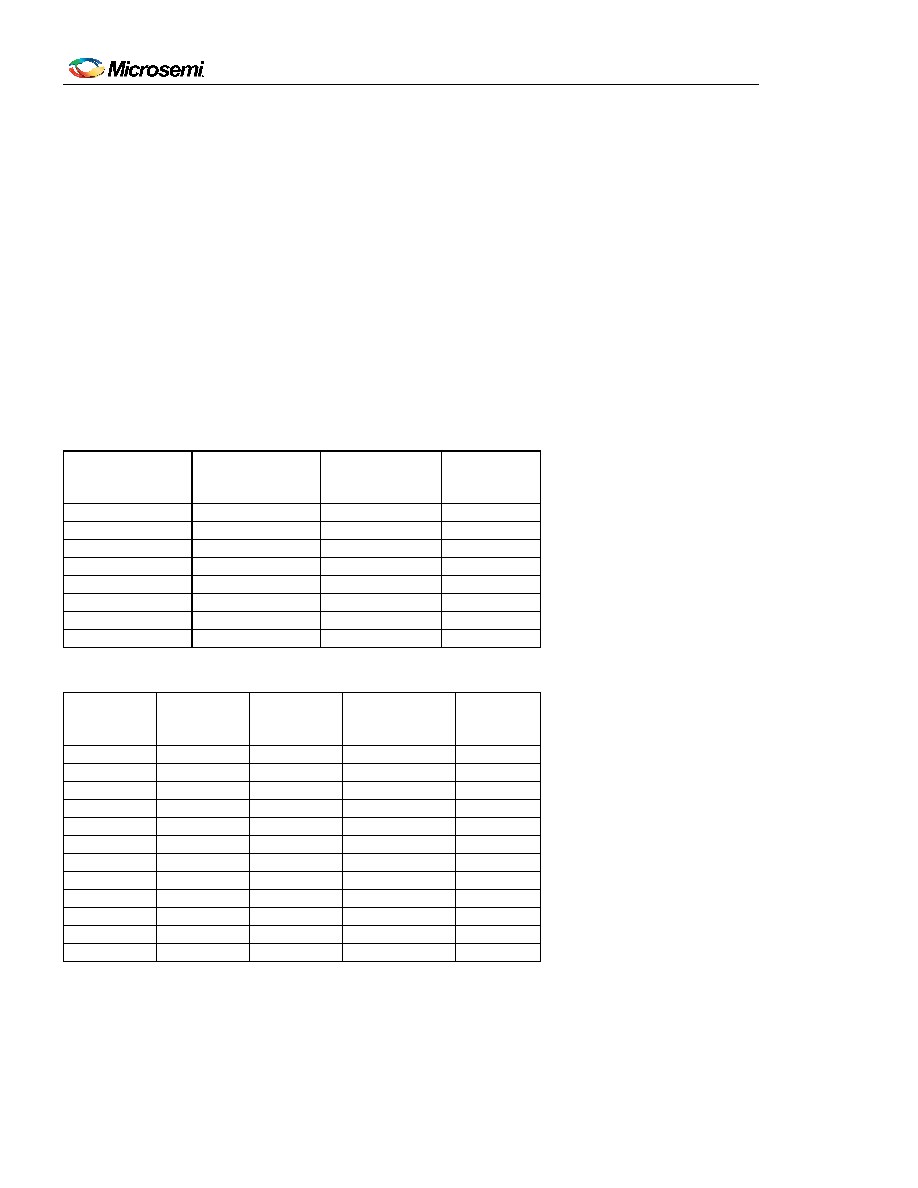
Table 7-6. Digital1 Frequencies
DIG1F[1:0]
SETTING IN
DIG1SS
SETTING IN
FREQUENCY
(MHz)
JITTER
(pk-pk, ns,
typ)
00
0
2.048
< 1
01
0
4.096
< 1
10
0
8.192
< 1
11
0
16.384
< 1
00
1
1.544
< 1
01
1
3.088
< 1
10
1
6.176
< 1
11
1
12.352
< 1
Table 7-7. Digital2 Frequencies
DIG2AF
SETTING
IN MCR6
DIG2F[1:0]
SETTING
IN MCR7
DIG2SS
SETTING
IN MCR6
FREQUENCY
(MHz)
JITTER
(pk-pk,
ns, typ)
1
00
0
6.312
< 1
1
10
0
10.000
<1
1
00
1
19.440
< 1
1
01
1
38.880
< 1
0
00
0
2.048
< 1
0
01
0
4.096
< 1
0
10
0
8.192
< 1
0
11
0
16.384
< 1
0
00
1
1.544
< 1
0
01
1
3.088
< 1
0
10
1
6.176
< 1
0
11
1
12.352
< 1
发布紧急采购,3分钟左右您将得到回复。
相关PDF资料
DS3231MZ+
IC RTC I2C 8SOIC
DS3231SN#T&R
IC RTC W/TCXO 16-SOIC
DS3232MZ+
IC RTC W/SRAM I2C 8SOIC
DS3232SN#T&R
IC RTC W/TCXO 20-SOIC
DS3234S#
IC RTC W/TCXO 20-SOIC
DS32C35-33#T&R
IC RTC ACCURATE I2C 3.3V 20-SOIC
DS3911T+
IC DAC 10BIT I2C QUAD 14TDFN
DS4000KI/WBGA
IC OSC TCXO 19.44MHZ 24-BGA
相关代理商/技术参数
DS3107FP000
制造商:Thomas & Betts 功能描述:30A,CON,2P3W,MG,107,125V
DS3107FRAB0
制造商:Thomas & Betts 功能描述:30A,REC,2P3W,MG,107,AB0,125,SC
DS3107MP000
制造商:Thomas & Betts 功能描述:30A,PLG,2P3W,MG,107,125V
DS3107MP00K
制造商:Thomas & Betts 功能描述:30A,PLG,2P3W,MG,107,125V,CC
DS3107MR000
制造商:Thomas & Betts 功能描述:30A,NLT,2P3W,MG,107,125V
DS3107MRAB0
制造商:Thomas & Betts 功能描述:30A,NLT,2P3W,MG,107,AB0,125V
DS3108A14S5S621
制造商:Amphenol Corporation 功能描述:
DS3108A14S6S
制造商:Amphenol Corporation 功能描述: